RFM95/96/97/98 shield library Part3

Register Read and Write

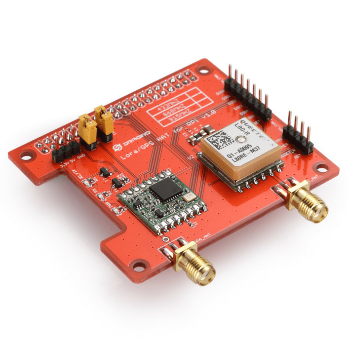
Now that I could reliably dump all the registers of the RFM9X shield I needed to be able to reset the Semtech 1276/7/8/9 back to factory settings (by strobing the reset pin) so the Rfm9XDevice class constructor gained an additional parameter, the reset GPIO pin.

To configure the RFM9X I wrote some wrapper functions to read/write byte values, word values and arrays of bytes. I found the TransferFullDuplex method didn’t work and I assume this was due to the non standard chip select pin usage.

Each method was tested by read/writing suitable register(s) in the device configuration (Needed to set it into LoRa mode first).

//---------------------------------------------------------------------------------
// Copyright (c) August 2018, devMobile Software
//
// Licensed under the Apache License, Version 2.0 (the "License");
// you may not use this file except in compliance with the License.
// You may obtain a copy of the License at
//
//     http://www.apache.org/licenses/LICENSE-2.0
//
// Unless required by applicable law or agreed to in writing, software
// distributed under the License is distributed on an "AS IS" BASIS,
// WITHOUT WARRANTIES OR CONDITIONS OF ANY KIND, either express or implied.
// See the License for the specific language governing permissions and
// limitations under the License.
//
//---------------------------------------------------------------------------------
namespace devMobile.IoT.Rfm9x.RegisterReadAndWrite
{
	using System;
	using System.Diagnostics;
	using System.Runtime.InteropServices.WindowsRuntime;
	using System.Threading.Tasks;
	using Windows.ApplicationModel.Background;
	using Windows.Devices.Spi;
	using Windows.Devices.Gpio;

	public sealed class Rfm9XDevice
	{
		private SpiDevice Rfm9XLoraModem;
		private GpioPin ChipSelectGpioPin;
		private const byte RegisterAddressReadMask = 0X7f;
		private const byte RegisterAddressWriteMask = 0x80;

		public Rfm9XDevice(int chipSelectPin, int resetPin)
		{
			SpiController spiController = SpiController.GetDefaultAsync().AsTask().GetAwaiter().GetResult();
			var settings = new SpiConnectionSettings(0)
			{
				ClockFrequency = 500000,
				Mode = SpiMode.Mode0,
			};

			// Chip select pin configuration
			GpioController gpioController = GpioController.GetDefault();
			ChipSelectGpioPin = gpioController.OpenPin(chipSelectPin);
			ChipSelectGpioPin.SetDriveMode(GpioPinDriveMode.Output);
			ChipSelectGpioPin.Write(GpioPinValue.High);

			// Factory reset pin configuration
			GpioPin resetGpioPin = gpioController.OpenPin(resetPin);
			resetGpioPin.SetDriveMode(GpioPinDriveMode.Output);
			resetGpioPin.Write(GpioPinValue.Low);
			Task.Delay(10);
			resetGpioPin.Write(GpioPinValue.High);
			Task.Delay(10);

			Rfm9XLoraModem = spiController.GetDevice(settings);
		}

		public Byte RegisterReadByte(byte address)
		{
			byte[] writeBuffer = new byte[] { address &= RegisterAddressReadMask };
			byte[] readBuffer = new byte[1];
			Debug.Assert(Rfm9XLoraModem != null);

			ChipSelectGpioPin.Write(GpioPinValue.Low);
			Rfm9XLoraModem.Write(writeBuffer);
			Rfm9XLoraModem.Read(readBuffer);
			ChipSelectGpioPin.Write(GpioPinValue.High);

			return readBuffer[0];
		}

		public ushort RegisterReadWord(byte address)
		{
			byte[] writeBuffer = new byte[] { address &= RegisterAddressReadMask };
			byte[] readBuffer = new byte[2];
			Debug.Assert(Rfm9XLoraModem != null);

			ChipSelectGpioPin.Write(GpioPinValue.Low);
			Rfm9XLoraModem.Write(writeBuffer);
			Rfm9XLoraModem.Read(readBuffer);
			ChipSelectGpioPin.Write(GpioPinValue.High);

			return (ushort)(readBuffer[1] + (readBuffer[0] << 8));
		}

		public byte[] RegisterRead(byte address, int length)
		{
			byte[] writeBuffer = new byte[] { address &= RegisterAddressReadMask };
			byte[] readBuffer = new byte[length];
			Debug.Assert(Rfm9XLoraModem != null);

			ChipSelectGpioPin.Write(GpioPinValue.Low);
			Rfm9XLoraModem.Write(writeBuffer);
			Rfm9XLoraModem.Read(readBuffer);
			ChipSelectGpioPin.Write(GpioPinValue.High);

			return readBuffer;
		}

		public void RegisterWriteByte(byte address, byte value)
		{
			byte[] writeBuffer = new byte[] { address |= RegisterAddressWriteMask, value };
			Debug.Assert(Rfm9XLoraModem != null);

			ChipSelectGpioPin.Write(GpioPinValue.Low);
			Rfm9XLoraModem.Write(writeBuffer);
			ChipSelectGpioPin.Write(GpioPinValue.High);
		}

		public void RegisterWriteWord(byte address, ushort value)
		{
			byte[] valueBytes = BitConverter.GetBytes(value);
			byte[] writeBuffer = new byte[] { address |= RegisterAddressWriteMask, valueBytes[0], valueBytes[1] };
			Debug.Assert(Rfm9XLoraModem != null);

			ChipSelectGpioPin.Write(GpioPinValue.Low);
			Rfm9XLoraModem.Write(writeBuffer);
			ChipSelectGpioPin.Write(GpioPinValue.High);
		}

		public void RegisterWrite(byte address, [ReadOnlyArray()] byte[] bytes)
		{
			byte[] writeBuffer = new byte[1 + bytes.Length];
			Debug.Assert(Rfm9XLoraModem != null);

			Array.Copy(bytes, 0, writeBuffer, 1, bytes.Length);
			writeBuffer[0] = address |= RegisterAddressWriteMask;

			ChipSelectGpioPin.Write(GpioPinValue.Low);
			Rfm9XLoraModem.Write(writeBuffer);
			ChipSelectGpioPin.Write(GpioPinValue.High);
		}

		public void RegisterDump()
		{
			Debug.WriteLine("Register dump");
			for (byte registerIndex = 0; registerIndex <= 0x42; registerIndex++)
			{
				byte registerValue = this.RegisterReadByte(registerIndex);

				Debug.WriteLine("Register 0x{0:x2} - Value 0X{1:x2} - Bits {2}", registerIndex, registerValue, Convert.ToString(registerValue, 2).PadLeft(8, '0'));
			}
		}
	}

	public sealed class StartupTask : IBackgroundTask
	{
		private const int ChipSelectLine = 25;
		private const int ResetLine = 17;
		private Rfm9XDevice rfm9XDevice = new Rfm9XDevice(ChipSelectLine, ResetLine);

		public void Run(IBackgroundTaskInstance taskInstance)
		{
			while (true)
			{
				rfm9XDevice.RegisterDump();

				Debug.WriteLine("Read RegOpMode (read byte)");
				Byte regOpMode = rfm9XDevice.RegisterReadByte(0x1);
				Debug.WriteLine("Preamble 0x{0:x2}", regOpMode);

				Debug.WriteLine("Set LoRa mode and sleep mode (write byte)");
				rfm9XDevice.RegisterWriteByte(0x01, 0b10000000); // 

				Debug.WriteLine("Read the preamble (read word)");
				ushort preamble = rfm9XDevice.RegisterReadWord(0x20);
				Debug.WriteLine("Preamble 0x{0:x2} - Bits {1}", preamble, Convert.ToString(preamble, 2).PadLeft(16, '0'));

				Debug.WriteLine("Set the preamble to 0x80 (write word)");
				rfm9XDevice.RegisterWriteWord(0x20, 0x80);

				Debug.WriteLine("Read the centre frequency (read byte array)");
				byte[] frequencyReadBytes = rfm9XDevice.RegisterRead(0x06, 3);
				Debug.WriteLine("Frequency Msb 0x{0:x2} Mid 0x{1:x2} Lsb 0x{2:x2}", frequencyReadBytes[0], frequencyReadBytes[1], frequencyReadBytes[2]);

				Debug.WriteLine("Set the centre frequency to 916MHz (write byte array)");
				byte[] frequencyWriteBytes = { 0xE4, 0xC0, 0x00 };
				rfm9XDevice.RegisterWrite(0x06, frequencyWriteBytes);

				rfm9XDevice.RegisterDump();

				Task.Delay(30000).Wait();
			}
		}
	}
}

The output of the application looked like this

Register dump
Register 0x00 – Value 0X00 – Bits 00000000
Register 0x01 – Value 0X09 – Bits 00001001
Register 0x02 – Value 0X1a – Bits 00011010
Register 0x03 – Value 0X0b – Bits 00001011
Register 0x04 – Value 0X00 – Bits 00000000
Register 0x05 – Value 0X52 – Bits 01010010
Register 0x06 – Value 0X6c – Bits 01101100
Register 0x07 – Value 0X80 – Bits 10000000
Register 0x08 – Value 0X00 – Bits 00000000
Register 0x09 – Value 0X4f – Bits 01001111
Register 0x0a – Value 0X09 – Bits 00001001
Register 0x0b – Value 0X2b – Bits 00101011
Register 0x0c – Value 0X20 – Bits 00100000
Register 0x0d – Value 0X08 – Bits 00001000
Register 0x0e – Value 0X02 – Bits 00000010
Register 0x0f – Value 0X0a – Bits 00001010
Register 0x10 – Value 0Xff – Bits 11111111
Register 0x11 – Value 0X70 – Bits 01110000
Register 0x12 – Value 0X15 – Bits 00010101
Register 0x13 – Value 0X0b – Bits 00001011
Register 0x14 – Value 0X28 – Bits 00101000
Register 0x15 – Value 0X0c – Bits 00001100
Register 0x16 – Value 0X12 – Bits 00010010
Register 0x17 – Value 0X47 – Bits 01000111
Register 0x18 – Value 0X32 – Bits 00110010
Register 0x19 – Value 0X3e – Bits 00111110
Register 0x1a – Value 0X00 – Bits 00000000
Register 0x1b – Value 0X00 – Bits 00000000
Register 0x1c – Value 0X00 – Bits 00000000
Register 0x1d – Value 0X00 – Bits 00000000
Register 0x1e – Value 0X00 – Bits 00000000
Register 0x1f – Value 0X40 – Bits 01000000
Register 0x20 – Value 0X00 – Bits 00000000
Register 0x21 – Value 0X00 – Bits 00000000
Register 0x22 – Value 0X00 – Bits 00000000
Register 0x23 – Value 0X00 – Bits 00000000
Register 0x24 – Value 0X05 – Bits 00000101
Register 0x25 – Value 0X00 – Bits 00000000
Register 0x26 – Value 0X03 – Bits 00000011
Register 0x27 – Value 0X93 – Bits 10010011
Register 0x28 – Value 0X55 – Bits 01010101
Register 0x29 – Value 0X55 – Bits 01010101
Register 0x2a – Value 0X55 – Bits 01010101
Register 0x2b – Value 0X55 – Bits 01010101
Register 0x2c – Value 0X55 – Bits 01010101
Register 0x2d – Value 0X55 – Bits 01010101
Register 0x2e – Value 0X55 – Bits 01010101
Register 0x2f – Value 0X55 – Bits 01010101
Register 0x30 – Value 0X90 – Bits 10010000
Register 0x31 – Value 0X40 – Bits 01000000
Register 0x32 – Value 0X40 – Bits 01000000
Register 0x33 – Value 0X00 – Bits 00000000
Register 0x34 – Value 0X00 – Bits 00000000
Register 0x35 – Value 0X0f – Bits 00001111
Register 0x36 – Value 0X00 – Bits 00000000
Register 0x37 – Value 0X00 – Bits 00000000
Register 0x38 – Value 0X00 – Bits 00000000
Register 0x39 – Value 0Xf5 – Bits 11110101
Register 0x3a – Value 0X20 – Bits 00100000
Register 0x3b – Value 0X82 – Bits 10000010
Register 0x3c – Value 0Xf1 – Bits 11110001
Register 0x3d – Value 0X02 – Bits 00000010
Register 0x3e – Value 0X80 – Bits 10000000
Register 0x3f – Value 0X40 – Bits 01000000
Register 0x40 – Value 0X00 – Bits 00000000
Register 0x41 – Value 0X00 – Bits 00000000
Register 0x42 – Value 0X12 – Bits 00010010
Read RegOpMode (read byte)
Preamble 0x09
Set LoRa mode and sleep mode (write byte)
Read the preamble (read word)
Preamble 0x08 – Bits 0000000000001000
Set the preamble to 0x80 (write word)
Read the centre frequency (read byte array)
Frequency Msb 0x6c Mid 0x80 Lsb 0x00
Set the centre frequency to 916MHz (write byte array)
Register dump
Register 0x00 – Value 0X54 – Bits 01010100
Register 0x01 – Value 0X80 – Bits 10000000
Register 0x02 – Value 0X1a – Bits 00011010
Register 0x03 – Value 0X0b – Bits 00001011
Register 0x04 – Value 0X00 – Bits 00000000
Register 0x05 – Value 0X52 – Bits 01010010
Register 0x06 – Value 0Xe4 – Bits 11100100
Register 0x07 – Value 0Xc0 – Bits 11000000
Register 0x08 – Value 0X00 – Bits 00000000
Register 0x09 – Value 0X4f – Bits 01001111
Register 0x0a – Value 0X09 – Bits 00001001
Register 0x0b – Value 0X2b – Bits 00101011
Register 0x0c – Value 0X20 – Bits 00100000
Register 0x0d – Value 0X01 – Bits 00000001
Register 0x0e – Value 0X80 – Bits 10000000
Register 0x0f – Value 0X00 – Bits 00000000
Register 0x10 – Value 0X00 – Bits 00000000
Register 0x11 – Value 0X00 – Bits 00000000
Register 0x12 – Value 0X00 – Bits 00000000
Register 0x13 – Value 0X00 – Bits 00000000
Register 0x14 – Value 0X00 – Bits 00000000
Register 0x15 – Value 0X00 – Bits 00000000
Register 0x16 – Value 0X00 – Bits 00000000
Register 0x17 – Value 0X00 – Bits 00000000
Register 0x18 – Value 0X10 – Bits 00010000
Register 0x19 – Value 0X00 – Bits 00000000
Register 0x1a – Value 0X00 – Bits 00000000
Register 0x1b – Value 0X00 – Bits 00000000
Register 0x1c – Value 0X00 – Bits 00000000
Register 0x1d – Value 0X72 – Bits 01110010
Register 0x1e – Value 0X70 – Bits 01110000
Register 0x1f – Value 0X64 – Bits 01100100
Register 0x20 – Value 0X80 – Bits 10000000
Register 0x21 – Value 0X00 – Bits 00000000
Register 0x22 – Value 0X01 – Bits 00000001
Register 0x23 – Value 0Xff – Bits 11111111
Register 0x24 – Value 0X00 – Bits 00000000
Register 0x25 – Value 0X00 – Bits 00000000
Register 0x26 – Value 0X04 – Bits 00000100
Register 0x27 – Value 0X00 – Bits 00000000
Register 0x28 – Value 0X00 – Bits 00000000
Register 0x29 – Value 0X00 – Bits 00000000
Register 0x2a – Value 0X00 – Bits 00000000
Register 0x2b – Value 0X00 – Bits 00000000
Register 0x2c – Value 0X00 – Bits 00000000
Register 0x2d – Value 0X50 – Bits 01010000
Register 0x2e – Value 0X14 – Bits 00010100
Register 0x2f – Value 0X45 – Bits 01000101
Register 0x30 – Value 0X55 – Bits 01010101
Register 0x31 – Value 0Xc3 – Bits 11000011
Register 0x32 – Value 0X05 – Bits 00000101
Register 0x33 – Value 0X27 – Bits 00100111
Register 0x34 – Value 0X1c – Bits 00011100
Register 0x35 – Value 0X0a – Bits 00001010
Register 0x36 – Value 0X03 – Bits 00000011
Register 0x37 – Value 0X0a – Bits 00001010
Register 0x38 – Value 0X42 – Bits 01000010
Register 0x39 – Value 0X12 – Bits 00010010
Register 0x3a – Value 0X49 – Bits 01001001
Register 0x3b – Value 0X1d – Bits 00011101
Register 0x3c – Value 0X00 – Bits 00000000
Register 0x3d – Value 0Xaf – Bits 10101111
Register 0x3e – Value 0X00 – Bits 00000000
Register 0x3f – Value 0X00 – Bits 00000000
Register 0x40 – Value 0X00 – Bits 00000000
Register 0x41 – Value 0X00 – Bits 00000000
Register 0x42 – Value 0X12 – Bits 00010010

The next step is to extract the SPI register access functionality into a module and configure the bare minimum of settings required to get the RFM9X to transmit.

RFM95/96/97/98 shield library Part2

Register Dump

Next step was to dump all registers (0x00 thru 0x40) of the SX1276/7/8/9 device

//---------------------------------------------------------------------------------
// Copyright (c) July 2018, devMobile Software
//
// Licensed under the Apache License, Version 2.0 (the "License");
// you may not use this file except in compliance with the License.
// You may obtain a copy of the License at
//
// http://www.apache.org/licenses/LICENSE-2.0
//
// Unless required by applicable law or agreed to in writing, software
// distributed under the License is distributed on an "AS IS" BASIS,
// WITHOUT WARRANTIES OR CONDITIONS OF ANY KIND, either express or implied.
// See the License for the specific language governing permissions and
// limitations under the License.
//
//---------------------------------------------------------------------------------
namespace devMobile.IoT.Rfm9x.RegisterScan
{
   using System;
   using System.Diagnostics;
   using System.Threading.Tasks;
   using Windows.ApplicationModel.Background;
   using Windows.Devices.Gpio;
   using Windows.Devices.Spi;

   public sealed class Rfm9XDevice
   {
      private SpiDevice rfm9XLoraModem;
      private GpioPin chipSelectGpioPin;

      public Rfm9XDevice(int chipSelectPin)
      {
         SpiController spiController = SpiController.GetDefaultAsync().AsTask().GetAwaiter().GetResult();
         var settings = new SpiConnectionSettings(0)
         {
            ClockFrequency = 500000,
            Mode = SpiMode.Mode0,
         };

         GpioController gpioController = GpioController.GetDefault();
         chipSelectGpioPin = gpioController.OpenPin(chipSelectPin);
         chipSelectGpioPin.SetDriveMode(GpioPinDriveMode.Output);
         chipSelectGpioPin.Write(GpioPinValue.High);

         rfm9XLoraModem = spiController.GetDevice(settings);
      }

      public Byte RegisterReadByte(byte registerAddress)
      {
         byte[] writeBuffer = new byte[] { registerAddress };
         byte[] readBuffer = new byte[1];
         Debug.Assert(rfm9XLoraModem != null);

         chipSelectGpioPin.Write(GpioPinValue.Low);
         rfm9XLoraModem.Write(writeBuffer);
         rfm9XLoraModem.Read(readBuffer);
         chipSelectGpioPin.Write(GpioPinValue.High);

         return readBuffer[0];
      }
   }

   public sealed class StartupTask : IBackgroundTask
   {
      private const int ChipSelectLine = 25;
      private Rfm9XDevice rfm9XDevice = new Rfm9XDevice(ChipSelectLine);

      public void Run(IBackgroundTaskInstance taskInstance)
      {
         while (true)
         {
            for (byte registerIndex = 0; registerIndex <= 0x42; registerIndex++)
            {
               byte registerValue = rfm9XDevice.RegisterReadByte(registerIndex);

               Debug.WriteLine("Register 0x{0:x2} - Value 0X{1:x2} - Bits {2}", registerIndex, registerValue, Convert.ToString(registerValue, 2).PadLeft(8, '0'));
            }

            Task.Delay(10000).Wait();
         }
      }
   }
}

The output of the application looked like this

Register 0x00 – Value 0X00 – Bits 00000000
Register 0x01 – Value 0X09 – Bits 00001001
Register 0x02 – Value 0X1a – Bits 00011010
Register 0x03 – Value 0X0b – Bits 00001011
Register 0x04 – Value 0X00 – Bits 00000000
Register 0x05 – Value 0X52 – Bits 01010010
Register 0x06 – Value 0X6c – Bits 01101100
Register 0x07 – Value 0X80 – Bits 10000000
Register 0x08 – Value 0X00 – Bits 00000000
Register 0x09 – Value 0X4f – Bits 01001111
Register 0x0a – Value 0X09 – Bits 00001001
Register 0x0b – Value 0X2b – Bits 00101011
Register 0x0c – Value 0X20 – Bits 00100000
Register 0x0d – Value 0X08 – Bits 00001000
Register 0x0e – Value 0X02 – Bits 00000010
Register 0x0f – Value 0X0a – Bits 00001010
Register 0x10 – Value 0Xff – Bits 11111111
Register 0x11 – Value 0X71 – Bits 01110001
Register 0x12 – Value 0X15 – Bits 00010101
Register 0x13 – Value 0X0b – Bits 00001011
Register 0x14 – Value 0X28 – Bits 00101000
Register 0x15 – Value 0X0c – Bits 00001100
Register 0x16 – Value 0X12 – Bits 00010010
Register 0x17 – Value 0X47 – Bits 01000111
Register 0x18 – Value 0X32 – Bits 00110010
Register 0x19 – Value 0X3e – Bits 00111110
Register 0x1a – Value 0X00 – Bits 00000000
Register 0x1b – Value 0X00 – Bits 00000000
Register 0x1c – Value 0X00 – Bits 00000000
Register 0x1d – Value 0X00 – Bits 00000000
Register 0x1e – Value 0X00 – Bits 00000000
Register 0x1f – Value 0X40 – Bits 01000000
Register 0x20 – Value 0X00 – Bits 00000000
Register 0x21 – Value 0X00 – Bits 00000000
Register 0x22 – Value 0X00 – Bits 00000000
Register 0x23 – Value 0X00 – Bits 00000000
Register 0x24 – Value 0X05 – Bits 00000101
Register 0x25 – Value 0X00 – Bits 00000000
Register 0x26 – Value 0X03 – Bits 00000011
Register 0x27 – Value 0X93 – Bits 10010011
Register 0x28 – Value 0X55 – Bits 01010101
Register 0x29 – Value 0X55 – Bits 01010101
Register 0x2a – Value 0X55 – Bits 01010101
Register 0x2b – Value 0X55 – Bits 01010101
Register 0x2c – Value 0X55 – Bits 01010101
Register 0x2d – Value 0X55 – Bits 01010101
Register 0x2e – Value 0X55 – Bits 01010101
Register 0x2f – Value 0X55 – Bits 01010101
Register 0x30 – Value 0X90 – Bits 10010000
Register 0x31 – Value 0X40 – Bits 01000000
Register 0x32 – Value 0X40 – Bits 01000000
Register 0x33 – Value 0X00 – Bits 00000000
Register 0x34 – Value 0X00 – Bits 00000000
Register 0x35 – Value 0X0f – Bits 00001111
Register 0x36 – Value 0X00 – Bits 00000000
Register 0x37 – Value 0X00 – Bits 00000000
Register 0x38 – Value 0X00 – Bits 00000000
Register 0x39 – Value 0Xf5 – Bits 11110101
Register 0x3a – Value 0X20 – Bits 00100000
Register 0x3b – Value 0X82 – Bits 10000010
Register 0x3c – Value 0Xff – Bits 11111111
Register 0x3d – Value 0X02 – Bits 00000010
Register 0x3e – Value 0X80 – Bits 10000000
Register 0x3f – Value 0X40 – Bits 01000000
Register 0x40 – Value 0X00 – Bits 00000000
Register 0x41 – Value 0X00 – Bits 00000000
Register 0x42 – Value 0X12 – Bits 00010010

I also started to refactor the code (extracting the Read functionality and format the output in both hexadecimal and binary (convert.ToString in base2 + padleft) to make comparison of register values with the datasheet easier.

The device was not in LoRa mode (Bit 7 of RegOpMode 0x01) so the next step was to read and write registers so I could change its configuration.

RFM95/96/97/98 shield library Part1

Register Read

Over the last couple of weeks I have been working on a Windows 10 IoT Core C# library for my Dragino LoRa GPS hat for Raspberry PI. I initially started with the Dragino.LoRa library but after some experimentation and hacking I decided to write my own library (which is usually not a good idea).

DraginoLoraGPSHat

I wanted a lightweight LoRa only library (hopefully possible to backport to .NetMF) which didn’t try to hide how the Semtech 1276 chip functioned, and in the future could be configured to work with other vendors’ shields (dragino, electronictricks, elecrow, m2m).

I’m also working on an RFM69 Raspberry PI shield based on an electronictricks PCB populated with a RFM69HCW so I figured the experience of building a library would be useful.

The first step was to build a basic universal windows platform (UWP) background task to confirm that I could reliably communicate with the shield over SPI bus by reading a single register value (RegVersion the silicon version specified in the vendor datasheet).

//---------------------------------------------------------------------------------
// Copyright (c) July 2018, devMobile Software
//
// Licensed under the Apache License, Version 2.0 (the "License");
// you may not use this file except in compliance with the License.
// You may obtain a copy of the License at
//
//     http://www.apache.org/licenses/LICENSE-2.0
//
// Unless required by applicable law or agreed to in writing, software
// distributed under the License is distributed on an "AS IS" BASIS,
// WITHOUT WARRANTIES OR CONDITIONS OF ANY KIND, either express or implied.
// See the License for the specific language governing permissions and
// limitations under the License.
//
//---------------------------------------------------------------------------------
namespace devMobile.IoT.Rfm9x.RegisterRead
{
   using System;
   using System.Diagnostics;
   using System.Threading.Tasks;
   using Windows.ApplicationModel.Background;
   using Windows.Devices.Gpio;
   using Windows.Devices.Spi;

   public sealed class StartupTask : IBackgroundTask
   {
      private const int ChipSelectLine = 25;
      private SpiDevice rfm9XLoraModem;

      public void Run(IBackgroundTaskInstance taskInstance)
      {
         // Have to setup the SPI bus with custom Chip Select line rather than std CE0/CE1
         SpiController spiController = SpiController.GetDefaultAsync().AsTask().GetAwaiter().GetResult();
         var settings = new SpiConnectionSettings(0)
         {
            ClockFrequency = 500000,
            Mode = SpiMode.Mode0,
         };

         GpioController gpioController = GpioController.GetDefault();
         GpioPin chipSelectGpioPin = gpioController.OpenPin(ChipSelectLine);
         chipSelectGpioPin.SetDriveMode(GpioPinDriveMode.Output);
         chipSelectGpioPin.Write(GpioPinValue.High);

         rfm9XLoraModem = spiController.GetDevice(settings);

         while (true)
         {
            byte[] writeBuffer = new byte[]{ 0x42 }; // RegVersion
            byte[] readBuffer = new byte[1];

            chipSelectGpioPin.Write(GpioPinValue.Low);
            rfm9XLoraModem.Write(writeBuffer);
            rfm9XLoraModem.Read(readBuffer);
            chipSelectGpioPin.Write(GpioPinValue.High);

            Debug.WriteLine("RegVersion {0:x2}", readBuffer[0]);

            Task.Delay(10000).Wait();
            }
         }
   }
}

The dragino shield has the chip select (also know as slave select) line connected to pin 25 rather than the usual CS0 (pin 24) & CS1 (pin 26) so it has to be manually strobed.

'backgroundTaskHost.exe' (CoreCLR: CoreCLR_UWP_Domain): Loaded 'C:\Data\Users\DefaultAccount\AppData\Local\DevelopmentFiles\RegisterRead-uwpVS.Debug_ARM.Bryn.Lewis\System.Diagnostics.Debug.dll'. Skipped loading symbols. Module is optimized and the debugger option 'Just My Code' is enabled.
RegVersion 12
RegVersion 12

Next step was to dump all the registers of the HopeRF module.